PHYS250H: Power Supply Project I
 For Fall 2014, I decided to continue my work under Professor James Battat with the dark matter detector and he suggested doing so under PHYS250H -- an independent study in the Physics Department -- in order to receive credit for it. However, the project portion of the course veered from work with the PCB I created earlier and towards design of a PCB power supply for his Spring class PHYS310 "Experimental Physics." The power supply was needed for an Electronics student lab, where a five-pin DIN draws in four voltage levels of +12V, -12V, +5V and GND for a solderless breadboard. The PCB I designed would use this connector to draw in the four voltage levels, filter for overcurrent and allow direct input into the rails of a solderless breadboard.
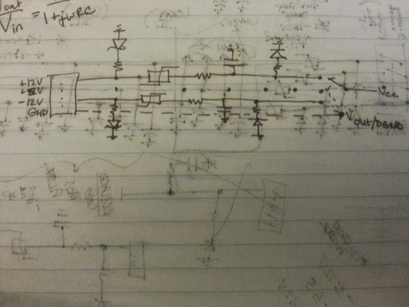
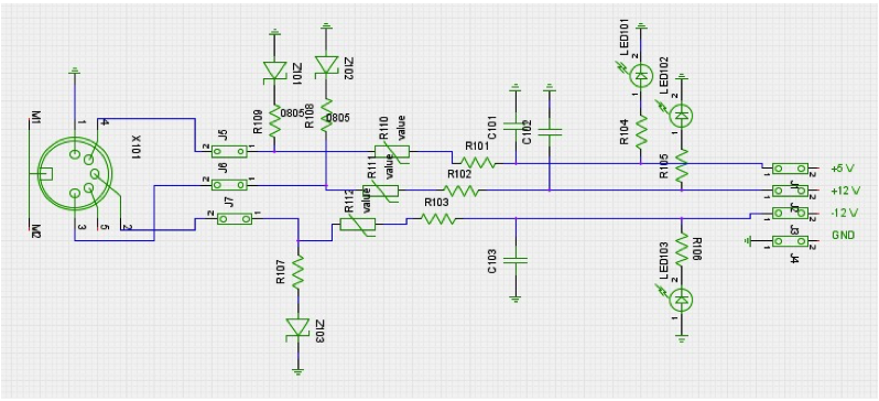
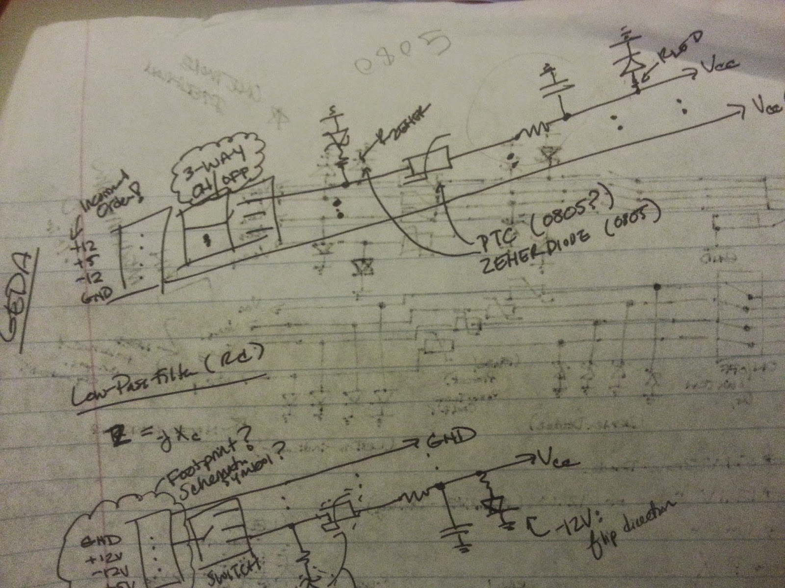
At the beginning of the process, Battat and I create a concept diagram demonstrating the overall flow of the power supply and, from it, a rough circuit diagram was generated. Over time, the schematic changed with additional and substitute components. A combination of resistors and capacitors create a low-pass filter and ensures that spikes in the voltage levels will not damage the circuit. Additionally, a zener diode is placed on each voltage line for fast-response protection against unexpected rises in voltage levels. A “positive temperature coefficient” (PTC) resistor will increase its resistance upon overloading or shorting of the load and will maintain high resistance until the overcurrent has been eliminated. The light emitting diodes (or LEDs) on each light serve as indication of successful and safe transmission between the connector and the jumper pins, which will allow for direct integration with the breadboard and other electronics. As a master on-off switch, a set of three jumpers can be used to connect and disconnect the power supply.
With these apsects in mind, I was able to use gEDA (again) to create a small PCB design that incorporated standard footprints and custom-made footprints (like the five-pin DIN connector). We had plans to send the PCB to OSH park -- which has incredible pricing for PCB fabrication.


Comments
Post a Comment